

From Sand to Smartphone: A Field Guide to the Electronics Stack
The essential guide to how electronic goods are made, layer by layer, for consumers, and industry newcomers.


Buckle up people, this is a long one. I’d say about once a day on LinkedIn I see a new iteration on a diagram designed to maximize likes, something mapping out “the semiconductor industry” and comparing companies like TSMC, Nvidia, and ASML by market cap. It’s not inherently bad, but it does a poor job of defining the flow of the industry, and it’s unclear who the diagram is directed at and what value it really brings.
It’s my hope that that’s not the case for this post. The Hidden Layer is all about pulling back the curtain on the inner workings of the world’s most critical industry for consumers and people who are not in the know.
This aims to be a touchpoint that I can reference in the future, a definitive piece that explores the depth and complexity of the world of semiconductors, microchips, and electronics, layer-by-layer, and explains WHY they are critical and what possible bottlenecks exist heading into 2026.
The purpose of this is to give readers a baseline to digest the news through- when you see an event (political, weather, or otherwise), you’ll have a framework for what it means and how it affects car prices, or delays on the new iPhone.
The classic example is an earthquake hitting Taiwan. Yes, it’s a huge concentration of semiconductor manufacturing, especially front-end fab sites. Yes, it could swiftly bring the global economy to a halt, or at least create some sleepless nights for supply chain operators (as it did in April 2024).
But as we’ve seen with China’s restrictions on rare earth mineral exports, or recent friction between the Netherlands and China over Nexperia, a maker of comparatively less cutting-edge chips (which are essential in many products), it takes a lot less than an earthquake to disrupt supply chains, and it could happen at literally any point in the process.
The stack begins with raw materials and moves its way up to finished goods. Let’s dig in.
1: Island of Chips (Front-End)
2: Packaging and OSAT (Back-End)
3: Copper Nervous System (PCB)
5: Middlemen of Stability (Distributors)
6: Architects of the Final Product (OEM)

Metro Mining barge with bauxite in Queensland, Australia. Image credit: Mining.com.au
LAYER 0: Dirt with Lawyers - Raw Materials & Processing
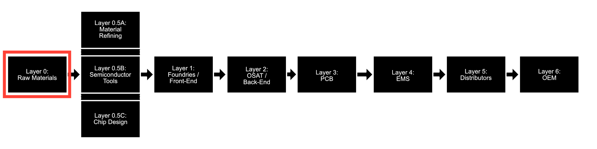
1. What this layer does:
This is where the electronics world begins, long before a wafer or a circuit board or even a transistor comes into view. The raw inputs of modern technology start as ordinary minerals pulled out of the ground and then pushed through layers of chemical processing until they become something usable. Examples:
Quartz becomes metallurgical silicon, which becomes polysilicon.
Bauxite becomes aluminum.
Rare earth ores become magnets and phosphors.
Lithium brines become battery-grade lithium salts.
None of this looks like electronics yet, but without this layer nothing further up the stack can exist.
2. What it touches:
Upstream is geology and mining. Downstream is everything else. Semiconductor fabs (layer 1) need hyper-pure polysilicon- arguably the most important but as we’ll see, these are all points of failure. Packaging houses (layer 2) need gold wire, copper, and molding compounds. PCB (layer 3) factories need copper foil, fiberglass, resins, and specialty chemicals. Even the cleanrooms depend on fluorinated gases, solvents, etchants, and ultrapure inputs coming from this layer. The entire electronics industry is downstream of a surprisingly small group of materials suppliers.
3. Who the major players are:
In polysilicon you have Hemlock Semiconductor in Michigan, Wacker Chemie in Germany, OCI in South Korea, and a collection of Chinese giants that dominate solar-grade output. In rare earth refining, China controls most of the midstream conversion steps, from ore to separated oxides to magnet precursors. For specialty chemicals you see names like Shin-Etsu, JSR, Merck, Linde, and Entegris. It’s an upstream world, but it is full of quietly important companies that determine what is possible further down the line.
4. Why this layer is a bottleneck in 2025:
The bottleneck is not the minerals themselves, it is the processing. Mining is distributed. Refining is not. Most critical materials pass through a handful of countries, and often one country. Polysilicon refining is energy-intensive and expensive, so capacity sits where electricity is cheap and environmental rules allow it. Rare earth separation is dominated by China because they built the refining ecosystem early and at scale. The geopolitical climate has turned this into a pressure point. Export controls on gallium, germanium, and graphite in 2023–2024 showed how easily upstream constraints can ripple into entire industries. Lead times for adding new refining capacity run into years, sometimes decades. The world keeps discovering new uses for these materials, but the ability to refine them has not kept pace.
5. Example disruption:
When China tightened export controls on gallium and germanium in 2023 and then expanded restrictions to include materials like graphite in 2024, it was a reminder that upstream pressure can move silently and suddenly. These are not glamorous elements, but they feed into RF semiconductors, photovoltaics, power electronics, and batteries. Overnight, companies from Europe to Japan were forced to assess their exposure, track inventories, and search for alternate refining sources. Nothing physically broke, no factory collapsed, and yet the entire downstream system felt the shock.
That’s the nature of Layer 0- it’s not as flashy as a natural disaster, but it’s the ground on which all the rest is built.
LAYER 0.5: The Hidden Architects — Materials Refiners, Toolmakers, and Chip Designers
Layer 0.5 is the semi-hidden region where upstream leverage quietly concentrates. These are companies that never touch your phone or laptop directly, yet everything you own depends on them. They sit between nature and the fab, and each one creates constraints that ripple through the whole system.
LAYER 0.5A: Materials Refining - Hemlock, Wacker, OCI
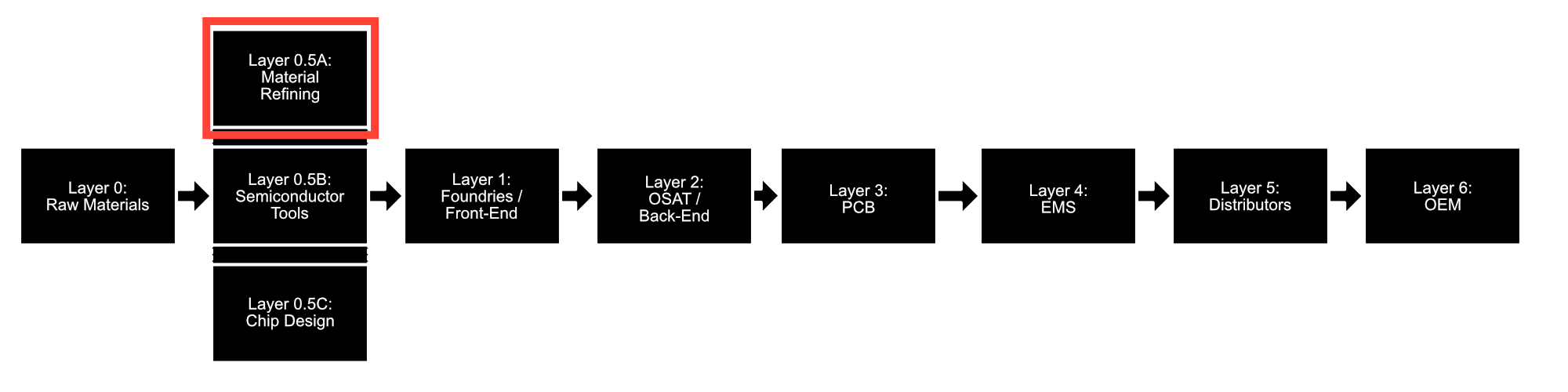
1. What this sublayer does:
We discussed this a bit before, but this is more of a focus on the processing. This is where minerals stop being rocks and start becoming usable inputs for semiconductor manufacturing. Refiners take quartz, metallurgical-grade silicon, or complex chemical precursors and push them through high-temperature, high-purity, high-energy conversion steps until they reach “electronics grade.” This is where the purity jumps from parts per million to parts per trillion.
2. What it touches:
Upstream: mining and chemical feedstocks.
Downstream: wafer manufacturers, solar ingot makers, and specialty chemical companies.
They are the hinge between geology and semiconductor physics.
3. Who the players are:
Hemlock Semiconductor (US), Wacker Chemie (Germany), OCI (South Korea), plus Chinese solar giants who dominate lower-purity output of polysilicon. A handful of companies globally can make true semiconductor-grade polysilicon, which makes this layer surprisingly concentrated.
If we think about Hemlock Semiconductor, in my backyard of Michigan, that’s America’s primary source of high-purity polysilicon. It’s one location, effectively in the middle of nowhere (not too far from Dow Chemical’s HQ). If that goes down, it’s a national security event for the US.
4. Why it is a bottleneck in 2025:
Refining is capital-intensive, energy-intensive, and slow to scale. Environmental rules and electricity prices determine where capacity sits. China’s dominance in many refining steps, plus export controls on materials like gallium and germanium, revealed how upstream chemical chokepoints can instantly affect multiple downstream sectors.
5. Example disruption:
China’s 2023–2024 gallium and germanium controls were a reminder that nothing here needs to “break” physically for the world to feel a shock. A policy change at the refining layer can squeeze RF chips, photovoltaics, and power devices overnight.
EUV (extreme ultraviolet) lithography machines, such as those made by ASML, are used to etch patterns onto silicon wafers. Image credit: Azo Nano/Shutterstock
LAYER 0.5B: Semiconductor Tools - ASML, Tokyo Electron, Lam Research, Applied Materials
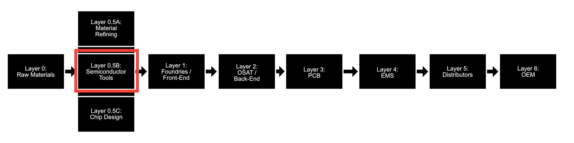
1. What this sublayer does:
These firms build the machines that make chips possible. Lithography, deposition, etch, metrology- everything in a fab runs through tools built by only a few companies. Famously, ASML’s EUV scanners are the most complex machines humans have ever manufactured.
2. What it touches:
Upstream: precision optics, lasers, specialty metals, and mechatronic subsystems.
Downstream: every wafer made at advanced nodes.
Without this sublayer, Layer 1 cannot even exist.
3. Who the players are:
ASML (EUV lithography), Tokyo Electron (deposition, etch), Lam Research (etch), Applied Materials (deposition, CMP), KLA (metrology). Each has near-monopoly control over an essential step.
4. Why it is a bottleneck in 2025:
Lead times for EUV tools stretch past a year. There is no alternative supplier. Export controls shape who is allowed to buy certain tools. A supply hiccup in a single optical subsystem in Veldhoven (Netherlands) can delay an entire fab’s ramp. This layer is one of the deepest strategic chokepoints in the global economy, and although ASML has become something of a household name in past years, it’s still one of the least known bottlenecks.
5. Example disruption:
The 2022–2023 semiconductor equipment export restrictions to China showed how geopolitics can essentially redraw the map of who may manufacture at what node. ASML’s technology has become a geopolitical artifact, not just an industrial tool.
At this point you may also see an emerging trend- export restrictions (usually by the US and EU) on goods to China- usually equipment -are countered by export restrictions on goods from China (usually raw materials). The goal of the US in this case is to restrict its own dependency on China for chips and the ability of China to gain more leverage. The goal of China is to counter that, maintain its moat, and to retain its position as the world’s manufacturer.
LAYER 0.5C: Chip Design - Nvidia, AMD, Apple Silicon, Qualcomm
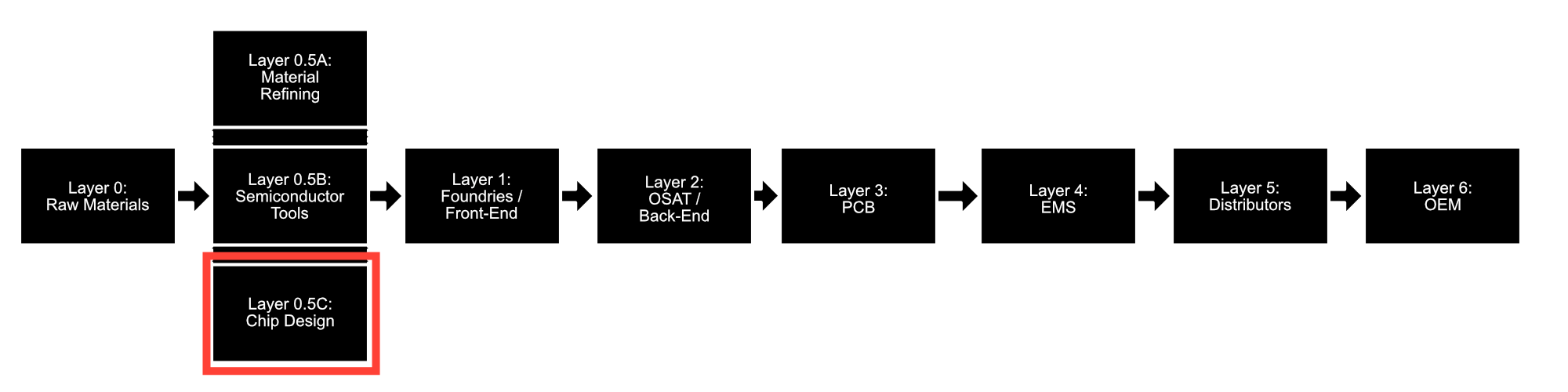
1. What this sublayer does:
Chip designers are the architects of computation. They do not manufacture chips themselves. They create the blueprints- GPUs, CPUs, modems, accelerators — that fabs turn into physical silicon. Modern design is an ecosystem of RTL engineering, verification, EDA tooling, IP licensing, and architectural breakthroughs.
This layer (within this framework) pertains only to fabless designers, who will typically rely on TSMC or Samsung for manufacturing (as we’ll see next layer). There are many players who both design and manufacture chips, such as Infineon, Texas Instruments, STMicroelectronics, and others. These firms often have a specialty in one category, such as analog, automotive, or power electronics, with some overlap between.
2. What it touches:
Upstream: EDA tools (Cadence, Synopsys), IP cores (Arm), memory interface standards, packaging roadmaps.
Downstream: fabs, OSATs, board-level integrators, entire industries built around their silicon.
3. Who the players are:
Nvidia in AI accelerators. Apple in mobile SoCs. AMD in CPUs and GPUs. Qualcomm in wireless. Even though they outsource manufacturing, these companies effectively determine the performance frontier for consumer and enterprise electronics.
4. Why it is a bottleneck in 2025:
The bottleneck here is architectural leadership. Demand for compute has exploded past the capacity of fabs to scale linearly. The result is that companies like Nvidia exert outsized influence on hardware design, software ecosystems, supply allocation, and manufacturing priorities. A single architecture decision- like memory bandwidth or packaging type -cascades through every downstream layer from HBM suppliers to EMS firms.
5. Example disruption:
Nvidia’s 2023–2024 GPU allocation crisis showed how a design-layer bottleneck can look identical to a manufacturing shortage. Demand outpaced packaging capacity, and the entire AI supply chain scrambled- not because fabs failed, but because the architectural center of gravity shifted faster than the physical world could adjust.
It’s worth noting that there are potential alternatives to traditional computing and digital ICs. I’ve covered Normal Computing’s development of the first thermodynamic chip, and there are other frontiers being explored, such as ultra-low power chips and reversible computing. These have the potential to upend the paradigm, and their impact would be most felt at this layer. I’ll look to dig into these in a future post.
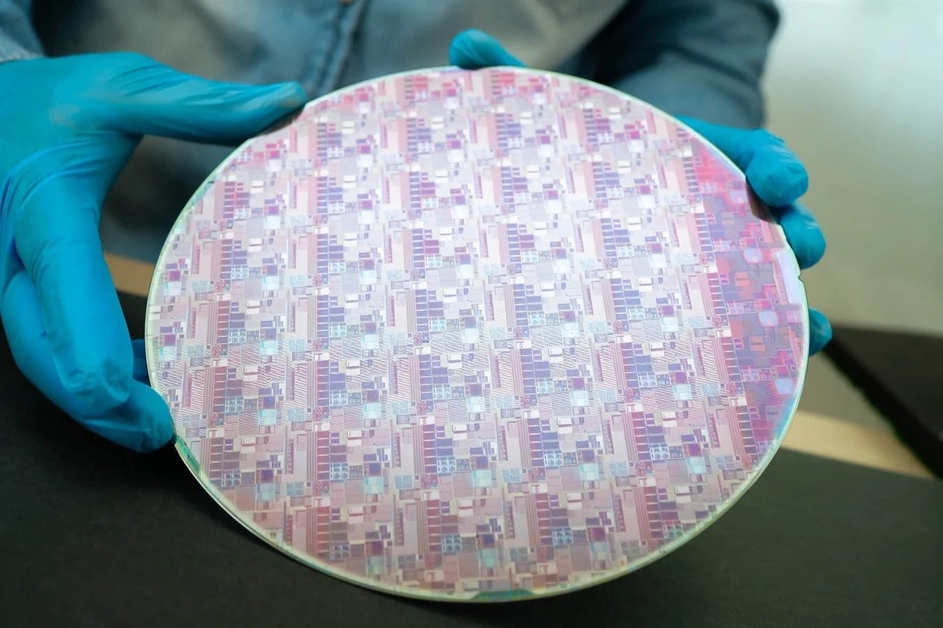
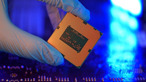
LAYER 1: The Island of Chips - Front-End Semiconductor Manufacturing
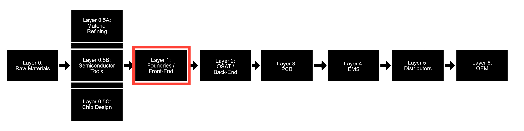
1. What this layer does:
This is where sand finally becomes computation. Front-end fabs take hyper-pure polysilicon, slice it into wafers, and then use an almost theatrical sequence of depositions, etches, ion implants, and photolithography steps to carve billions of transistors into silicon. A modern fab is closer to a physics experiment than a factory. Everything here happens at atomic scales, in cleanrooms that scrub the air a thousand times cleaner than a hospital, inside tools that cost as much as skyscrapers. This is the layer that turns raw materials into the digital brain of every device we own.
2. What it touches:
Upstream, they rely on the refined materials from Layer 0- polysilicon, specialty gases, photoresists, copper, and exotic chemicals produced by a handful of firms. They also rely on equipment monopolies like ASML’s EUV tools, Tokyo Electron deposition systems, and Lam’s etch platforms. Downstream, every single electronics layer depends on what comes out of a fab. If Layer 0 is geology with lawyers, Layer 1 is physics with billion-dollar price tags. Nothing downstream can substitute or work around a shortage of chips at a given node.
3. Who the major players are:
TSMC is the gravitational center of advanced logic. Samsung sits beside them at the cutting edge, with Intel rebuilding its footing. For mature nodes you see companies like GlobalFoundries (USA), UMC (Taiwan), and SMIC (China). Each has its own process technology and capabilities, but only a few- TSMC and Samsung in particular- can build the high-performance processors that drive AI accelerators, smartphones, and data centers. The geographic clustering is stark. So much of the world’s leading-edge logic sits on one island and one peninsula.
4. Why this layer is a bottleneck in 2025:
The fragility here comes from concentration. Advanced logic is overwhelmingly produced in Taiwan and South Korea. EUV lithography- the tool you need to make cutting-edge chips- is produced by a single Dutch company (ASML, as discussed). The cleanroom ecosystem is so specialized that recreating these fabs elsewhere is a decade-long challenge. Even small disruptions matter. A brief power sag can ruin wafers worth tens of millions of dollars. More broadly, demand for high-performance computing has ripped past the industry’s pace of capacity additions. Even with CHIPS Act incentives, the world cannot simply “build another TSMC” on demand. The barrier is not money, it is know-how, supply chains, and time.
5. Example disruption:
When the Hualien earthquake hit Taiwan in 2024, it jolted the world’s most important semiconductor cluster. TSMC paused operations, evacuated cleanrooms, and inspected tool stability. Some wafer cycles were interrupted mid-process, which effectively destroys them. Even a temporary outage forced customers across automotive, compute, and industrial sectors to run recalculations on supply assumptions. Nothing catastrophic happened, but the episode was a reminder of how thin the margins are. If you shake the island where the world keeps its most advanced fabs, you feel it everywhere else. It takes only hours of downtime to ripple through quarters of production planning downstream.
A microchip after packaging and OSAT.
LAYER 2: The Bottleneck Next Door - Advanced Packaging and OSAT
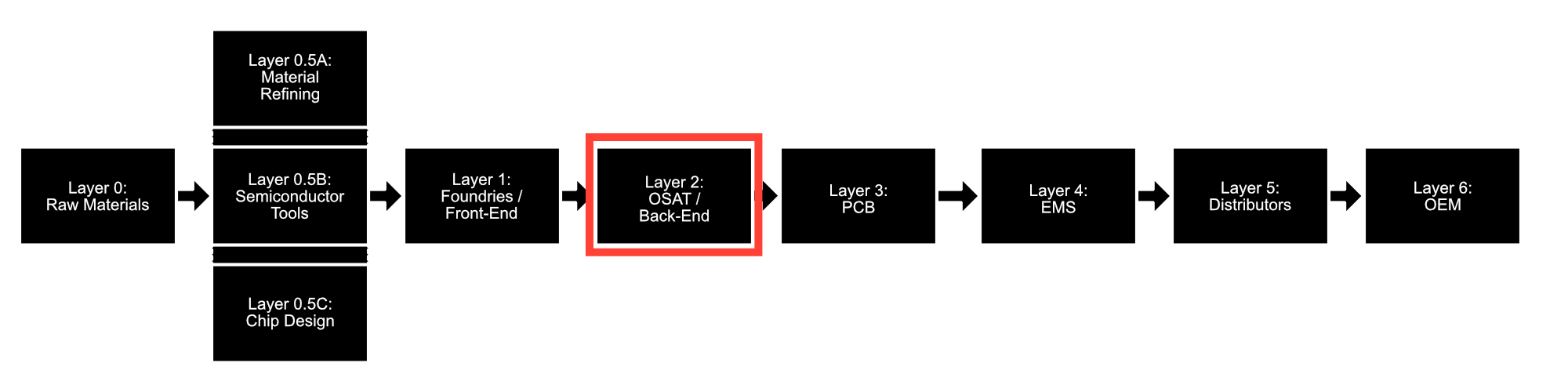
1. What this layer does:
Once a wafer leaves the fab, it is still useless. The dies have no protection, no electrical contacts, and no way to be handled, tested, or assembled. Advanced packaging is the stage where individual chips are cut from the wafer, bonded to substrates, wired, encapsulated, tested, sorted, and prepared for real-world use. This includes everything from basic wire bonding to cutting-edge 2.5D and 3D integration, chiplets, interposers, and high-bandwidth memory (HBM) stacks. If the front-end is physics, packaging is precision carpentry and electrical engineering fused together. It is the bridge between silicon and the rest of the world.
Traditionally, packaging and OSAT has been a lower-cost activity that was outsourced to countries that could support volume at a lower cost. However, this has changed somewhat in recent years as packaging has become more complex to suit needs for mobile devices and data centers.
2. What it touches:
Upstream, they receive bare dies from fabs, often still fragile and untested. They rely on substrates, molding compounds, underfill materials, copper, gold wire, and tooling that has its own supply constraints. Downstream, they feed into PCB assembly, module integrators, EMS firms, and ultimately OEMs. Packaging is the connective tissue. If a fab makes the brain, packaging provides the skull, nerves, and skin that allow it to function.
3. Who the major players are:
The giants here are ASE Group, SPIL (Siliconware), Amkor, JCET, and Powertech. On the more advanced end, TSMC and Samsung have moved aggressively into high-end packaging to support chiplet architectures and AI accelerators. This is also where you see major substrate manufacturers- Ibiden, Shinko, Unimicron — and where cutting-edge packaging increasingly lives inside the same geographic footprint as the fabs they serve.
4. Why this layer is a bottleneck in 2025:
Historically, packaging was treated as low-margin, low-glamour work and was offshored accordingly. But that strategic assumption collapsed the moment AI demand exploded. AI chips require massive bandwidth and thermals that only advanced packaging can deliver. Suddenly, OSAT capacity became the new scarcity, especially for substrate-based 2.5D and HBM-intensive designs. The world realized that it could build more wafers, but without somewhere to package them, the bottleneck simply moved downstream. Add geographic concentration- much of the world’s advanced packaging sits in Taiwan- and you get a layer that looks mundane on paper but is now one of the most strategically constrained parts of the electronics stack.
Packaging and OSAT is a particularly unique vulnerability for national defense for countries not in Asia (where it is heavily concentrated, more than any other piece of the equation- in part due to the cost-sensitive nature of packaging). The US in particular only has about 5% of global OSAT volume within its borders.
5. Example disruption:
When the Hualien earthquake shook Taiwan in 2024, the immediate headlines focused on fab downtime. But packaging houses were hit too. Facilities paused operations for inspections, tool stability checks, and safety protocols. Even temporary disruptions here create subtle but far-reaching ripples: chip testing delayed, substrate deliveries pushed out, downstream module builds paused. These delays do not always show up in the news, but they show up in lead times. This is the quiet vulnerability of Layer 2. It exists in the seam between silicon and the supply chain, and when that seam shifts, the entire product schedule shifts with it.
LAYER 3: The Copper Nervous System - PCB and PCBA Manufacturing
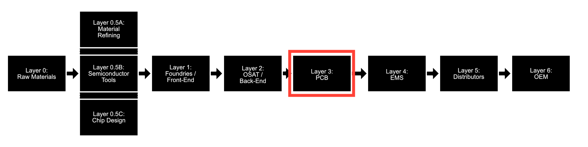
1. What this layer does:
If chips are the brains, printed circuit boards are the nervous system. A PCB is a stack of copper and fiberglass that routes power and signals between components. PCBA- printed circuit board assembly -is the step where components are placed, soldered, inspected, and transformed into functional modules. This is where electronics truly take shape. Every device, from a laptop to an EV to a dishwasher, passes through this layer. It is ordinary compared to fabs and packaging, but it carries the full weight of the industry. No board, no product.
There is intentionally some overlap between this step and the next, where EMS firms will typically own PCBA (but not PCB) manufacturing, and often higher-level assembly as well.
2. What it touches:
Upstream, this layer depends on copper foil, resins, laminates, solder paste, stencils, and a stream of components from distributors and semiconductor houses. It also relies on precise machinery: pick-and-place robots, reflow ovens, x-ray inspection, SPI and AOI systems. Downstream, PCBs and PCBAs flow into EMS factories, automotive modules, telecom base stations, consumer electronics assembly lines, and thousands of industrial applications. Nearly everything that gets built touches this layer, even if only for a few seconds on a pick-and-place line.
3. Who the major players are:
On the fabrication side, you see companies like Unimicron, Compeq, Tripod, and Ibiden. In Southeast Asia, Vietnamese and Thai facilities have become essential for medium- and high-volume builds. On the PCBA side, the ecosystem ranges from massive EMS firms handling assembly internally to regional specialists like Jabil (which does both), Pegatron, Sanmina, and a constellation of mid-sized assemblers that keep industrial and automotive sectors running. It is a sprawling, distributed network, but with geographic clusters that matter a lot.
4. Why this layer is a bottleneck in 2025:
PCB fabrication is heavily concentrated in China, with Taiwan, South Korea, Thailand, and Vietnam handling much of the rest. Environmental rules, cost structure, and decades of accumulated know-how mean there is very little capacity in the US or Europe. PCBA is equally clustered in Asia, especially for high-volume consumer devices. These clusters make the system efficient but fragile. A flood, a power outage, or a lockdown in just one region can delay millions of units downstream. And unlike chips or packaging, PCBs are low dollar-value items with long lead times and limited fungibility. You cannot easily replace a specific board with a similar one. The design is the design. If it is delayed, everything above it waits.
5. Example disruption:
During Vietnam’s COVID shutdowns in 2021, factories producing everything from PCBs to assembled boards were forced into extended closures. This hit global electronics in a way that surprised many observers. Suddenly, laptop makers, automotive suppliers, and even consumer appliance manufacturers found themselves short of basic PCB assemblies. These were not cutting-edge semiconductors. They were everyday boards. Yet the absence of a $3 PCB halted $500 devices. It revealed a structural truth: the industry has built extraordinary resilience around chips and components, but far less around the humble board. It’s the layer you only think about when it stops.

Smartphone PCBA. The PCB (previous layer) is visible underneath the components. Image credit: Best Technology Co., Ltd. (bestpcbs.com)
LAYER 4: The Megafactories - EMS and Final Assembly
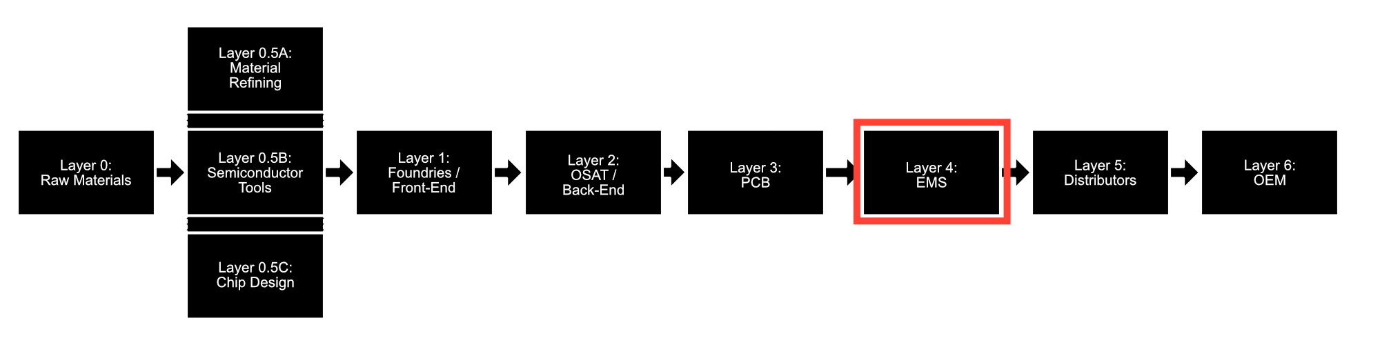
1. What this layer does:
Electronics Manufacturing Services (EMS) firms are the places where all the upstream complexity finally comes together. Chips, substrates, PCBAs, displays, batteries, connectors, plastics, antennas- everything lands on their production lines and becomes a finished product. These factories run at staggering scale. Phones, laptops, routers, wearables, automotive modules, medical devices, and industrial controllers all move through EMS lines in some form. If Layer 3 provides the nervous system, Layer 4 builds the body. This is where supply chains stop being abstract and become physical objects.
I’ve created this with a bit of overlap- typically “EMS” will refer to much of the previous step, PCBA assembly, and sometimes add batteries or other electronics, or even build the finished good.
2. What it touches:
Upstream, they depend on every layer you have discussed so far: semiconductors, packaging houses, PCB fabricators, distributors, mechanical suppliers, and an ocean of components. They also rely on logistics networks to keep thousands of part numbers flowing on a just-in-time cadence. Downstream, they feed into OEMs and brands who add the final software, testing, customer packaging, and global distribution. An EMS firm is the central junction where engineering, procurement, forecasting, and operations collide.
3. Who the major players are:
Foxconn (Hon Hai) towers over the landscape, assembling everything from iPhones to servers. Pegatron, Wistron, Luxshare, BYD Electronics, Jabil, Flex, Celestica, and Sanmina form the rest of the global backbone. Some OEMs like Samsung or Dell do part of their own assembly, but for the most part, EMS firms are the industrial muscle behind modern electronics. They run campuses the size of small cities, with hundreds of thousands of workers, robot cells, SMT lines, injection molding, machining centers, subassembly plants, and in-house logistics.
4. Why this layer is a bottleneck in 2025:
Scale is both their strength and their fragility. High-volume assembly is concentrated in a few countries- China above all, with Vietnam, Thailand, Malaysia, Mexico, and India growing but not yet equivalent. Labor availability, local policy shifts, energy costs, and public health disruptions all hit this layer hard. OEMs often have less visibility into EMS capacity constraints than they assume. A line cannot be conjured out of thin air during a surge. Certifications, tooling, line design, worker training, and quality systems take months to establish. When allocation hits here, it is not components being rationed, it is physical space and human bandwidth.
5. Example disruption:
In late 2022, Foxconn’s Zhengzhou facility- the world’s largest iPhone assembly site -faced extended lockdowns and labor unrest. Output dropped sharply. Apple issued rare public warnings about delays. What looked like a local labor-health event became a global electronics story within days. Phones, accessories, and downstream retail inventories were affected. This was the EMS bottleneck in full view: a single megafactory, specializing in a single family of products, is a point of enormous leverage. When it stumbles, the world notices immediately. Unlike chip shortages, which are invisible to consumers, EMS failures show up on store shelves.
To me, the EMS is the sweet spot of electronics that’s just 1 tier below OEMs, easy for consumers to understand (the PCBA is large and visible and tangible), and it’s also a piece that explains how so much of the modern world comes together. PCBAs are not a commodity, but they lean more that way than other parts of the ecosystem. EMS firms hold a large part of the market, and are the backbone on which modern electronics are built.
LAYER 5: The Middlemen of Stability - Component Distribution
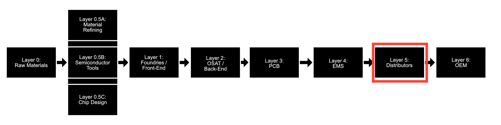
1. What this layer does:
Component distributors are the quiet infrastructure behind the electronics economy. They sit between manufacturers and the thousands of OEMs, EMS firms, and engineering teams who need a constant flow of parts. On paper, they buy and resell components, but in reality they perform a dozen hidden functions: credit extension, inventory buffering, lifecycle management, demand smoothing, obsolescence forecasting, kitting, and design-in support. They are a mix of bank, logistics firm, and consultant. Without them, the system would be volatile to the point of failure.
2. What it touches:
Upstream, distributors work with semiconductor manufacturers, passive component makers, interconnect suppliers, and the entire long tail of electronics suppliers. Downstream, they feed every type of customer: consumer electronics, EVs, industrial controls, aerospace, medical devices, telecom, and all the EMS and PCBA plants that sit one layer below OEMs. They synchronize information and material in a way no OEM can replicate individually. In shortages, they become the rationing authority. In gluts, they become the shock absorber.
3. Who the major players are:
Globally, the key names are Arrow, Avnet, and Future. There are also smaller firms that specialize in high-mix, low-volume (helpful for prototyping), such as Digi-Key, Mouser, and Farnell, as well as some that focus specifically on Asia. Regionally, there are dozens of smaller specialists servicing automotive, aerospace, or industrial niches. These firms collectively manage staggering catalogs- millions of SKUs with constantly shifting lead times, lifecycle stages, and demand curves. They are the ecosystem that translates chaos into availability, or at least predictability.
If everything up to this point represents engineering, design, and manufacturing excellence, distributors represent the market side, which is unbelievably complex in its own right.
4. Why this layer is a bottleneck in 2025:
Demand is volatile, product lifecycles are shortening, and semiconductor supply remains uneven across nodes. When the bullwhip effect hits- late visibility, panic ordering, double-booking, cancellations -distributors are the ones who absorb the shock. But they are not infinitely elastic. Once inventory tightens, allocation rules kick in and customers discover how little visibility they truly have into the upstream system. The complexity of modern BOMs, the pace of product updates, and the reality of geopolitical constraints mean that even large OEMs cannot forecast accurately without distributor partnership. The bottleneck is not only physical components, it is information precision.
5. Example disruption:
During the 2020–2022 automotive chip crisis, demand forecasting errors converged with pandemic shutdowns and soaring semiconductor lead times. Automakers cancelled orders early and then tried to reorder at massive volume six months later- right when consumer electronics demand was surging. Distributors found themselves caught between fabs with no spare capacity and OEMs asking for allocations they could not fulfill. The result was cascading shortages across everything from microcontrollers to power MOSFETs to simple analog parts. A single missing $1 automotive-grade IC could halt a $40,000 vehicle. This was the bullwhip made visible, and it revealed how much stability depends on distributors being able to read the market before the market reads itself.

Smartphones, tablets, and laptops are prime examples of products shipped by OEMs that are heavily PCBA and component-dependent. These are classic examples, but there are infinite others.
LAYER 6: The Architects of the Final Product - OEMs and System Integrators
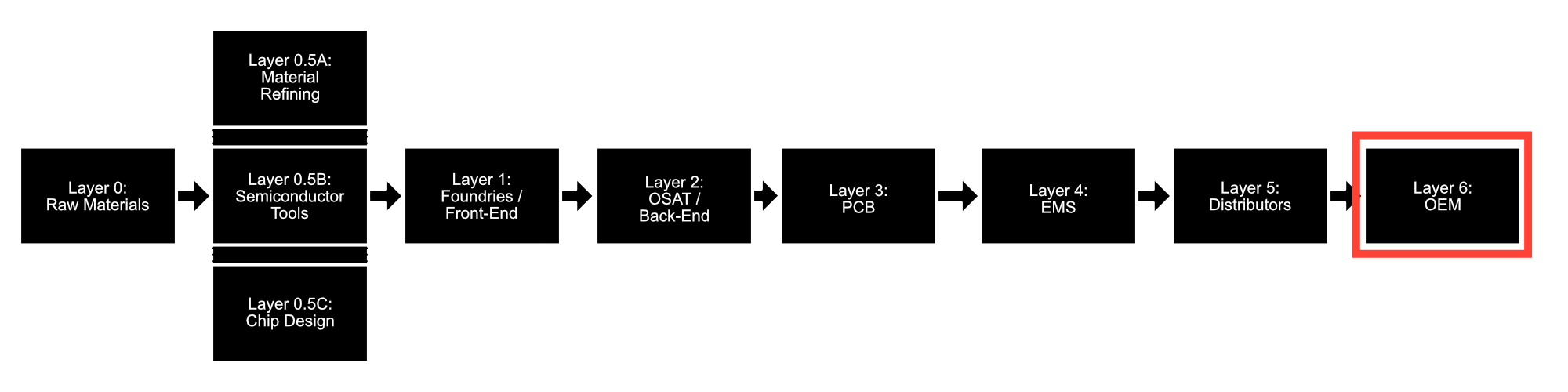
1. What this layer does:
OEMs transform assembled electronics into finished, coherent products. They decide what gets built, what performance matters, what technologies are worth integrating, and how thousands of components turn into a device people recognize and trust. They orchestrate design, firmware, mechanical engineering, regulatory compliance, quality assurance, supplier selection, and forecasting. A phone, an inverter, a medical device, a tractor, a router -all of them begin as decisions made at this layer about architecture, cost, and time to market. This is where technology is shaped into something that can be sold.
2. What it touches:
Upstream, OEMs depend on every preceding layer: distributors for parts, EMS firms for assembly capacity, PCB and substrate houses for boards, OSATs for packaged chips, fabs for silicon, materials refiners for inputs, and sometimes even raw material markets when risks rise. Downstream, they touch retail channels, regulatory regimes, after-sales support, and entire end-use industries. The OEM is where technical choices become business consequences. A thermal limit on a chip, a substrate shortage, a PCB footprint change, or a late firmware fix can alter the entire production calendar.
3. Who the major players are:
Apple, Tesla, Dell, Cisco, Siemens, Bosch, Sony, and thousands of industrial and automotive OEMs that never trend on social media but build critical infrastructure. In many ways, the most influential OEMs today are those who blend hardware with software ecosystems- Apple with its end-to-end silicon strategy, Tesla with over-the-air updates and in-house chips, Cisco with integrated networking stacks. These firms do not simply buy parts, they shape the direction of entire supply chains through their architectural decisions.
When you think of OEMs, it can be helpful to think beyond the classic examples (i.e. Apple and Samsung)- every consumer electronic, appliance, vehicle, or piece of industrial equipment is produced by an OEM.
4. Why this layer is a bottleneck in 2025:
The fragility here comes from complexity and decision speed. OEMs forecast demand imperfectly, often with long feedback loops. They redesign products faster than suppliers can adjust. They push for cost reductions while demand for performance rises. They often do not have deep visibility beyond tier 1 suppliers (although this is changing with new tools), which means disruptions at layers 2, 3, or 5 arrive as surprises even when upstream signals existed for months. And because OEMs place the largest and most visible orders, their forecasting errors can propagate downstream as panic, bullwhip, or overcorrection. This layer is not fragile because of shortage alone, it is fragile because the entire stack is shaped by decisions made here under uncertainty.
5. Example disruption:
When the automotive chip crisis unfolded, OEMs realized that their long-favored “just-in-time” procurement strategies offered little resilience. A single microcontroller shortage shut down assembly lines across the US, Europe, and Asia. Factories producing complex products were halted not by labor or metal, but by the absence of a chip small enough to fit on a thumbnail. In another sphere, Apple’s struggle to manage its assembly footprint during the 2022–2023 period demonstrated how even the most sophisticated OEM can be exposed when a megafactory stumbles. Redesigns, alternative sourcing, and emergency engineering changes all flowed from disruptions they did not fully see coming. The vulnerability here is not technical, it is systemic: the OEM sits at the intersection of everything, and when that intersection clogs, there is no easy detour.
Wrapping Things Up
You’ve made it to the end, so let’s keep things short and sweet. When people think of “electronics”, they probably picture something like a circuit board assembly, and to most consumers, the actual manufacturing processes and materials are completely unknown. That’s understandable, because of the level of complexity is so high that it may as well be meaningless to most people.
But in a world that is increasingly defined by electronics, both economically and in how we live our daily lives, I think it’s essential for consumers to at least have a primer or a framework to filter the news through.
Hopefully you took that away from this lengthy post. I’m sure I’ll refer back to it as we continue to explore industry bottlenecks and tech advances, and these 7 layers (plus 3) will become part of an ongoing series exploring this industry.